内蒙古分析电镜英文
- tem电镜样品
- 2024-04-27 17:00:24
- 450
fib芯片提供维修、系统安装、技术升级换代、系统耗材,以及应用开发和培训。

Electron microscopy, also known as electron microscopy, is an important field in materials science and technology. It is a non-invasive imaging technique that allows researchers to visualize and study the structures and properties of materials at the atomic scale. In this article, we will provide an overview of the history of electron microscopy, its applications, and the techniques used in this field.
The history of electron microscopy dates back to the 1930s when scientists first discovered that light could be used to create an image of a material. However, it was not until the 1950s that electron microscopy emerged as a viable technique for studying materials. One of the most significant breakthroughs in electron microscopy was the development of the transmission electron microscope (TEM) in 1988. This microscope allowed researchers to obtain high-resolution images of materials and to study their properties at the atomic scale.
Electron microscopy has many applications in materials science and technology. It is widely used for studying the microstructure and properties of metals, semiconductors, and insulators. For example, electron microscopy can be used to study the crystal structure of materials, to determine the electronic properties of materials, and to study the physical properties of materials such as conductivity and optical properties.
The techniques used in electron microscopy include several advanced imaging techniques such as:
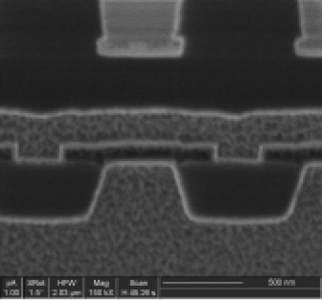
1. Scanning electron microscopy (SEM): SEM is a widely used technique that involves accelerating a beam of electrons through a sample, which creates an image of the material's surface. SEM can be used to study the surface structure of materials and to study the chemical composition of materials.
2. Transmission electron microscopy (TEM): TEM is a technique that involves passing a beam of electrons through a thin slice of a material and detecting the images on a screen. TEM is used to study the internal structure of materials and to study the properties of materials at the atomic scale.
3. Atomic force microscopy (AFM): AFM is a technique that involves using a sharp probe to scan the surface of a material and to study the properties of materials at the atomic scale. AFM can be used to study the surface structure of materials, to determine the chemical composition of materials, and to study the properties of materials such as conductivity and optical properties.
4. Confocal microscopy: Confocal microscopy is a technique that involves using a laser to create an image of a material and to study the properties of materials at the atomic scale. Confocal microscopy can be used to study the internal structure of materials and to study the properties of materials such as conductivity and optical properties.
In conclusion, electron microscopy is an important field in materials science and technology. It is a non-invasive imaging technique that allows researchers to visualize and study the structures and properties of materials at the atomic scale. The techniques used in this field include several advanced imaging techniques such as scanning electron microscopy, transmission electron microscopy, atomic force microscopy, and confocal microscopy. These techniques have many applications in materials science and technology and are widely used in research and industry.

下一篇
电镜扫描英文